Energy conversion and clean energy production using photoelectrochemical devices (PEC)
The DSSCs represent an alternative and simple, though complex, third generation photovoltaic tool that seeks to help solve global and environmental energy problem. It is recalle
d that the first generation devices are based on crystalline silicon and used in the common photovoltaic panels, while those of the second generation (“thin film” technologies) are used in the current amorphous silicon panels, CIGS, CdTe. Third generation devices, potentially, could exceed the limitations of predecessors and are based, for example, on organic photovoltaics, on polymeric cells, on those based on quantum dots, on DSSC, which are able to provide a cost of production / efficiency of photoconversion more advantageous.
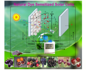
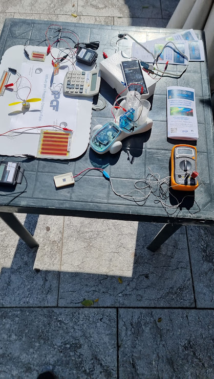
DSSCs use uncomplicated materials, do not require sophisticated preparation techniques, are close to eco-sustainability and are basically made up of:
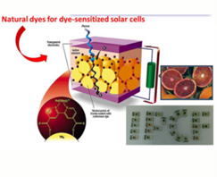
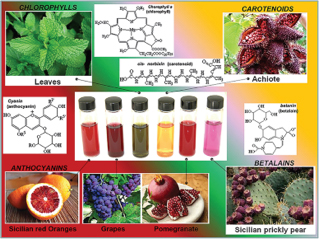
- a photoanode, a fundamental component useful for the collection of light energy, formed by a conductive glass (FTO) on which titania nanocrystals are deposited and subsequently sensitized, by simple immersion in a dye solution of synthetic origin (for example Ruthenium compounds ) or natural (anthocyanins, betalains, carotenoids, porphyrins, etc.), thi
s step is referred to as chemiadsorption; - an electrolytic mediator, i.e., a solution generally composed of suitable solvents and additives where iodine and its salts are dissolved;
- a cathode, or counterelectrode (CE), which always uses FTO bearing basically Platinum nanoparticles (Pt);
- a sealant useful for coupling the two electrodes and isolating them from the outside.
- a photoanode, a fundamental component useful for the collection of light energy, formed by a conductive glass (FTO) on which titania nanocrystals are deposited and subsequently sensitized, by simple immersion in a dye solution of synthetic origin (for example Ruthenium compounds ) or natural (anthocyanins, betalains, carotenoids, porphyrins, etc.), thi
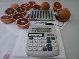
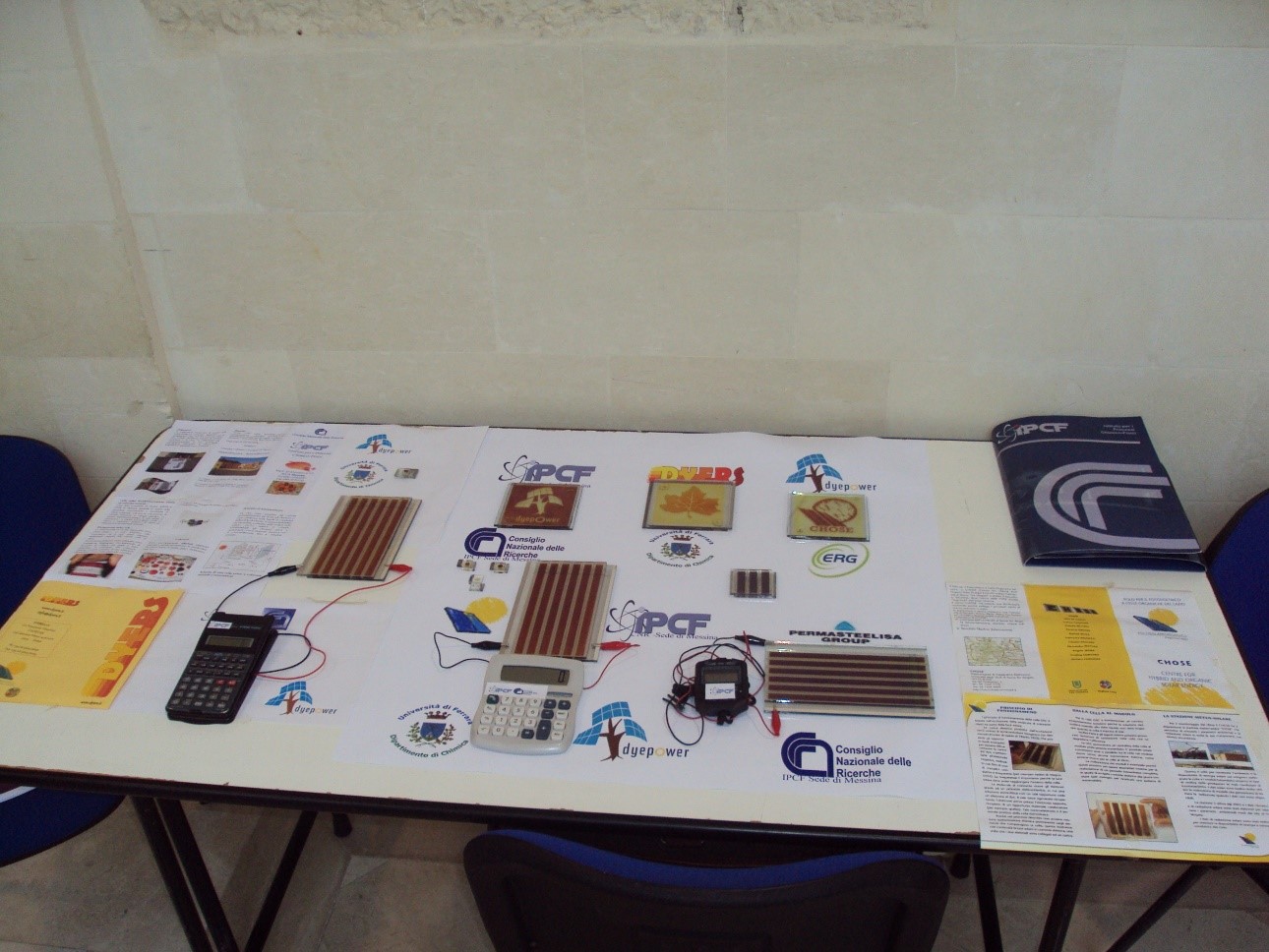
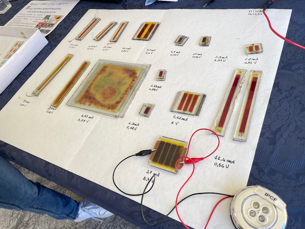
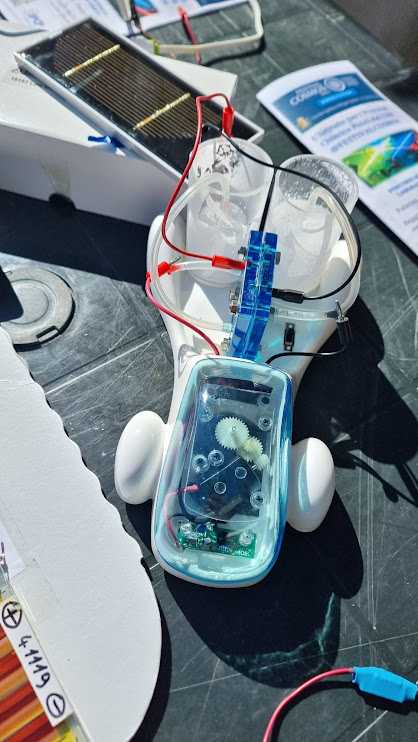
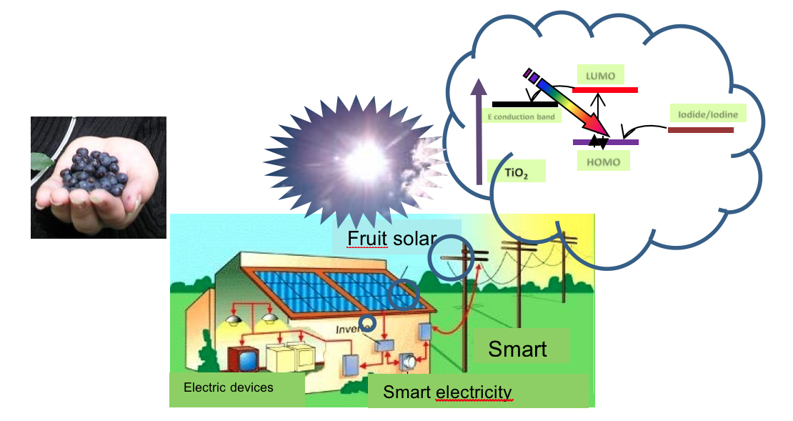
 The photoelectrochemical mechanism that takes place within them is the following: the dye absorbs the photons provided by the light that induce an electronic transition to a higher energy level, thus facilitating the transfer to the titania (semiconductor) that, in turn and thanks in the presence of FTO, transfers the electrons to the EC. If a load (lamp) is interposed between the two electrodes, the flow of electrons performs work (the lamp turns on). At this point the dye has oxidized (it has yielded electrons) and to resume its functionality it needs to be reduced (to reacquire the electrons); this function is carried out by the EC that thanks to the presence of the catalyst (Pt) accelerates the electrons passes to the electrolyte where it meets iodine, which is reduced to iodide and, in turn, gives the electrons received to the dye making it ready to start another photolithic cycle (an oxidation-reductive equilibrium is always established. The photoconversion reached in the cell (active area ~ 1cm2) was close to 13% and from this we started to create modules (consisting of several cells connected together in series or parallel) for applications that may require voltages and / or currents most important (5/12 V, 50/500 mA).
 The objective of the groups in IPCF working on this subject is to follow the fundamental study carried out in the laboratory, the realization of devices that are reliable over time with low production costs. These “tools” best perform their action in the indoor environment as they respond satisfactorily in conditions of diffused light and could be produced without engaging a fine technology; essentially an eco-friendly, reliable tool with indoor efficiencies close to 10% for uses in home automation, sensors, low cost objects, internet of things.
The Solare group works actively to develop technologies in accordance with the national strategy on hydrogen outlined in the National Recovery and Resilience Plan (PNRR) and in line with the position, widespread at European level, which identifies green hydrogen as one of the priority solutions in medium term for the decarbonisation of the energy system for sustainable mobility. In this regard, studies are focused on the development of non-critical materials and components for photoelectrolysis cells in tandem configuration for the direct conversion of solar energy into hydrogen and advanced systems for catalytic splitting assisted by solar and thermal energy and production of liquid carriers of hydrogen obtained from the photochemical and photoelectrochemical conversion of CO2 and water (AdP H2 project).
Furthermore, collaborations are active to develop third generation devices that use natural dyes from local products and biomass made with bacteria and fungi to power the sensors of a photovoltaic greenhouse created at the headquarters.
Another important project followed by the SOLARE group is linked to the The National Quantum Science and Technology Institute (NQSTI), NQSTI is a consortium that team up Italian entities carrying out competitive and innovative research in the field of quantum science and technology (QST), and will stimulate future industrial innovation in this field, providing a forum in which novel ideas and opportunities are transferred to companies. In order to ensure a long-term positive effect on the Italian economic growth and development, the whole innovation chain was considered: from the strengthening and coordination of the low-TRL research, to its translation into prototypes, favouring interfacing with industrial needs thanks to strong outreach and continued-education programs. In particular , IPCF activities will be Quantum Solar Cells design with quantum nanosystems (perovskite, 2D, quantum dots, etc.).
 Metal-halide perovskite-based tandem solar cells show great promise for overcoming the Shockley–Queisser single-junction efficiency limit via low-cost tandem structures, but so far, they employ conventional bottom-cell materials that require stringent processing conditions. Meanwhile, difficulty in achieving low-bandgap (<1.1 eV) perovskites limits all-perovskite tandem cell development.
Here we propose a tandem cell design based on a halide perovskite top cell and a chalcogenide colloidal quantum dot (CQD) bottom cell, where both materials provide bandgap tunability and solution processability. A theoretical efficiency of 43% is calculated for tandem-cell bandgap combinations of 1.55 (perovskite) and 1.0 eV (CQDs) under 1-sun illumination.
As part of the FOE project entitled “The raw materials of the future from non-critical, residual and renewable sources (FutuRaw) which was financed by the DSCTM Department, the Solare group carries out activities that involve the use, recycling, the design and production of new products and materials from alternative raw materials: non-critical raw materials and residues, and secondary raw materials. The activities are aimed at valorising non-edible biomass in the energy, environmental and cultural heritage sectors. In particular, the reuse of non-edible waste biomass as sensitizing dyes for third generation photovoltaics it will allow the development of fermentation strategies for the cultivation of microorganisms capable of producing natural pigments and the optimization and design processes of new DSSCs devices.
