Research topics:
Advanced Materials -Chemistry for Cultural Heritage – Chemistry for Life Sciences – Energy – Green Chemistry
Keywords:
Morphologic characterization, Microscopy, Nanostructured Materials, Thin Film deposition, EDS
Contact person:
Other info:
The laboratory deals with the morphological, structural, and compositional characterization of materials at different dimensional scales. The Transmission Electron Microscope (TEM) allows the analysis of the morphological properties (dimensions, shape, and distribution) of nanostructured materials such as nanoparticles, heterostructures, hybrid materials and assembled systems at the nanoscale, prepared by chemical synthesis. The Scanning Electron Microscope (SEM FEG) allows the large-scale characterization of different types of materials and surfaces with resolutions of tens of nanometers while the EDS system allows obtaining information on the composition of the investigated materials. In addition, magnetron sputter deposition of Au or Cr thin films and carbon layers via thermal evaporation is available for the preparation of non-conductive SEM samples. The laboratory is also equipped with a laminar flow hood for sample preparation.
LIST OF AVAILABLE INSTRUMENTATION
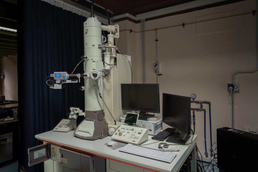
Transmission electron microscope (TEM) JEOL JEM-1010 with operating voltage ranging from 40kV to 100kV, for life science and material science applications. Operation Modes in Bright Field and Dark Field, magnification up to 500,000X, resolution of 0.45nm point to point. The microscope is equipped with a CCD camera for digital image acquisition and a EDX system (Energy Dispersive X-Ray Spectroscopy) to identify the elemental composition of materials.
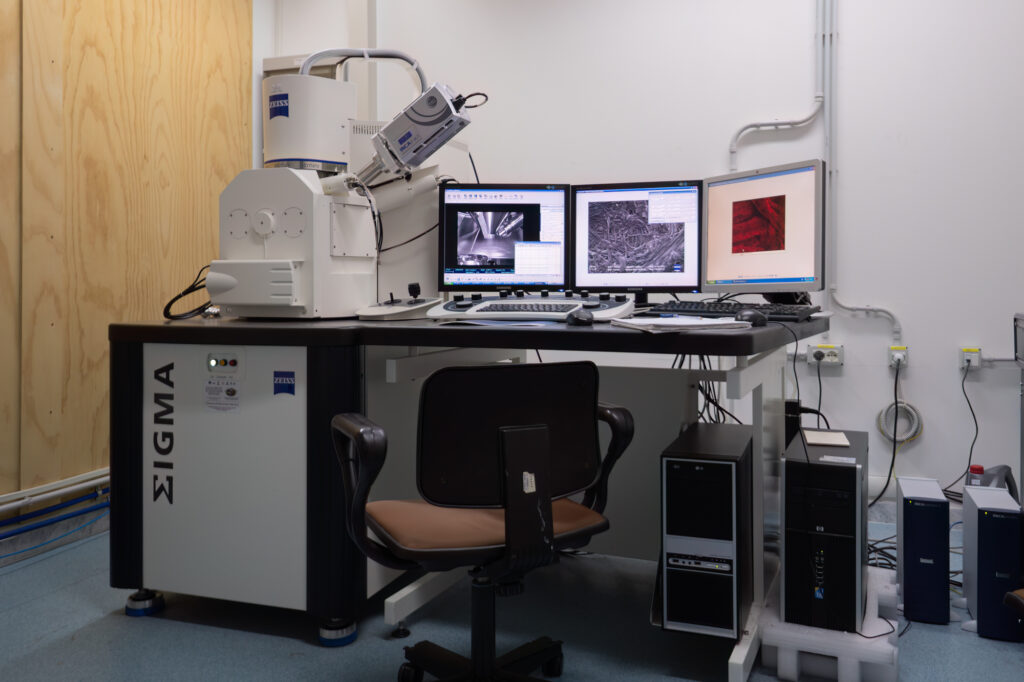
High-resolution scanning electron microscope (SEM) with field emission gun SIGMA ZEISS. The Gemini objective lens design combines electrostatic and magnetic fields to maximize optical performance while reducing field influences at the sample to a minimum. enabling excellent imaging, even on challenging samples such as magnetic materials. The microscope allows an efficient signal collection detecting secondary (SE) and/or backscattered (BSE) electrons. The maximum resolution can reach ~1nm. The SEM is equipped with energy-dispersive X-ray spectroscopy (EDS) system that for sample element analysis.
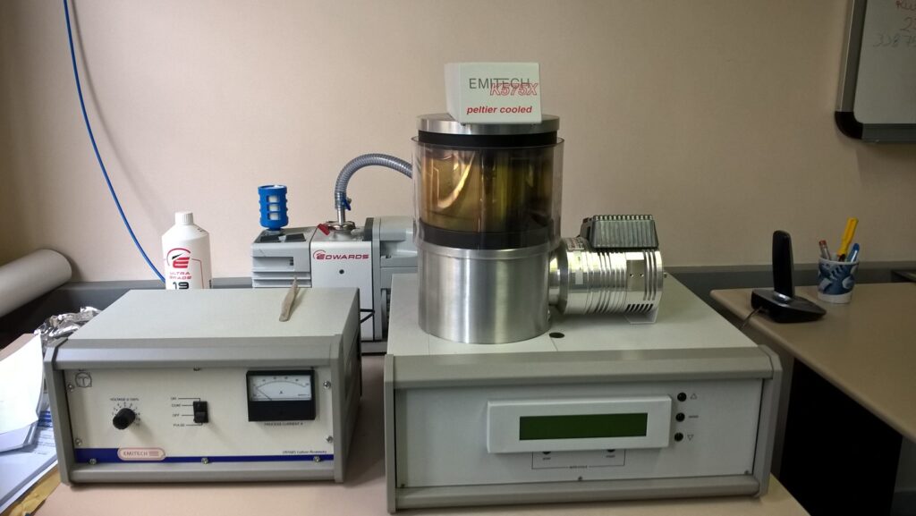
K575X Quorum sputter coater featuring a Peltier-cooled sputter head that enables fine coating (Cr Grain Size in the order of 0.5 nm) and thin film deposition (typically 5-10 nm) of metals for preparation of non-conductive SEM samples. The system is equipped with a rotating sample holder, Cr and Au targets, a microbalance for measuring the deposited thickness and allows multilayered depositions.